Technique that is sometimes used for a Printed Circuit Board Manufacturer UK is to print etch-resistant ink onto a PCB using a silkscreen process.
Multi-layer printed circuit boards
With the increasing complexity of electronic circuits, it is not always possible to provide all the necessary connections using only two sides of the PCB manufacture. This happens quite often in the design of high-density microprocessors and other similar boards.
The production of multilayer PCBs, although using the same processes as for single-layer boards, requires significantly more precision and control of the manufacturing process.
The boards are made from much thinner individual boards, one for each layer, and then glued together to form an overall PCB. As the number of layers increases, the individual boards must become thinner so that the finished PCB does not become too thick.
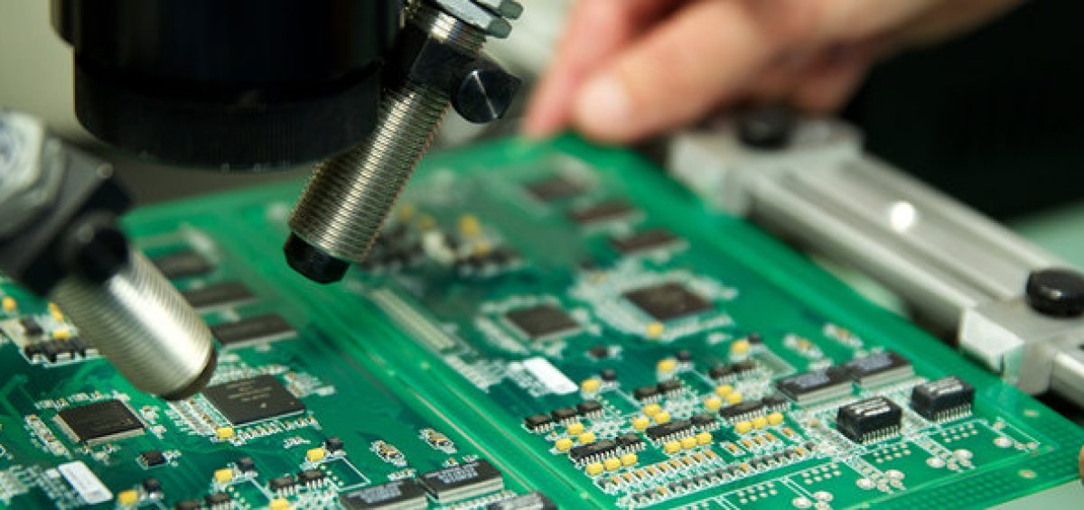
PCB holes and Vias
Holes often referred to as vias, are needed inside a PCB to connect different layers at different points. Holes may also be required to install PCB pinned components. Besides, some mounting holes may be required.
Typically, the inner surfaces of the holes have a copper layer so that they electrically connect the layers of the board. These “electroplated through holes” are manufactured using an electroplating process. This way you can connect the layers of the board.
It may be necessary for some holes to exist only in the center of the board, for example, when it is necessary to connect the inner layers of the board. These blind vias are drilled into their respective layers before the PCB layers are glued together.
PCB Solder plating and solder resist
When soldering a printed circuit board, it is necessary to protect the non-solder able areas with a layer of the so-called soldering resist. The addition of this layer helps prevent unwanted short circuits on PCBs caused by solder. Solder resist usually consists of a polymer layer and protects the board from solder and other contaminants. The color of the resist solder is usually dark green or red.
So that components added to the board, lead or SMT can be easily soldered to the board; the exposed portions of the board are usually tinned or plated with solder. Sometimes planks or sections of planks can be plated with gold. This may be applicable if some copper fingers will be used for edge connections.
PCB silkscreen
It is often necessary to print text and place other small printable elements on the PCB. This can aid in board identification, as well as marking component locations to aid troubleshooting, etc. The silkscreen created by PCB design software is used to add markings to the board after other manufacturing processes have been completed for the empty board completed.
PCB prototype
As part of any development process, it is generally a good idea to create a prototype before moving on to full production. It’s the same with PCBs, where a PCB prototype is usually made and tested before full production. However, it is always wise to stick as close to the final PCB manufacturing process as possible to ensure that few changes and few new elements are made to the final PCB.
It is about complexity and the number of materials and processes involved in making your flex PCB done. Flex PCB UK manufacturing has the same rigid PCB steps in addition to other ones.
The PCB manufacturing process is an essential element of the electronics manufacturing lifecycle. Many new areas of technology are used in the manufacture of printed circuit boards, which has significantly improved both the reduction in the size of the components and guides used and the reliability of the boards.
The process behind creating a reliable PCB involves precise layering, drilling, and testing to ensure flawless circuit performance. Modern manufacturers use advanced techniques to enhance durability and efficiency. For brands seeking visibility in the electronics industry, advertise with us to reach a targeted audience.